There are many industries that have various industry standards. These are often relevant to the internal workings of the industry, not something customers see, and help then industry work smoothly as a whole. This is particularly important when various parts of the industry need to interact with a range of suppliers and clients. Sometimes the standards are based on standards bodies or even a regulator, sometimes industry bodies, sometimes simply the de facto standard of the major player.
But sometimes when you get under the hood you can be shocked to find a lack of industry standard where clearly one would be both obvious and simple.
Now, when I explain this latest craziness, I know, for sure, someone will come out of the woodwork and say "but there is standard X". The problem is that whatever standard here may be it is clearly not widely used in the industry as yet.Also, when I explain this latest craziness, someone will say, "Why not just make a standard then?". Well, see xkcd/927. Obviously I could propose a standard - this is a very simple matter, but there is no way I could get it adopted. I'd go for all in one JSON file to be honest.
PCB Assembly files
The issue is PCB assembly files. I am (personally) quite new to this, and discussing with my colleagues that do this for a living they are "Oh, yeh, it is crap, there is no standard".
What is needed...
When making a printed circuit board, and adding components (assembled PCB), you need a few things.
- The actual artwork for the printed circuit board - several bits, such as the copper layers, the solder resist, solder paste, the silk screen, the edge cuts, the drill file.
- The details of the components you need placing on the board
- The details of exactly where those components are to go on the board
There are actually a load of other things, some of which are fabricator specific, like PCB thickness (and number of layers, and material), solder resist colour, silk screen colour, copper thickness and finish, and various production options. If an extensible standard existed (e.g. JSON or even XML) it could include a load of "common" attributes and allow for custom attributes, and so allow ordering a PCB to be literally loading one file. I have been caught out forgetting one of the many options before now and managed to get a board the wrong thickness. My PCB package knows the thickness but has no way to include that in the production files.
Artwork
The first part does seem to be pretty standard, though it sort of evolved, but now is quite good - GERBER files and drill files all in a zip file. There are several options and versions, but in general these really "just work". Even details like whether coordinates are based on inches of millimetres are standard headers in the file now. It seems a variety of de facto / proprietary standards have congealed in to something pretty common at last.
Picking components
Picking the components is the area I would expect to be complicated, but I was quite surprised. My experience here is of two PCB fabrication companies, one in UK and one in China. To my surprise, in both cases, they were able to track down components quite easily.
The basic parameters of "Manufacturer name" and "Manufacturer part number" seem to cover it very well, but even without these - even something simple like calling a component "5k1" and stating a package of "0603" will get you a standard tolerance 0603 package 5.1 kΩ resistor. Indeed, on one occasion whilst trying to find the part for an inductor, I totally failed to find it on the parts site, but it turned out that simply putting the value and package "4x4" found one that I failed to find.
Comma Separated Value
One of the issues is the file format, something obvious for standardisation, seems totally arbitrary. The only common factor seems to be the use of CSV files.
In one case the web site allowed me to load the CSVs from the PCB drawing package, display it spreadsheet style, and then let me select which rows are which things (Bill of Materials, and Positions), and then select which columns in those rows are things like "Manufacturer name", "Part number", and so on, with some level of pre-guessing in place. This is a total faff as every time you load the files you have to go through this process.
In another case the fabricator specify the exact set of columns to use for each file. This has the advantage that if you can make a script to make the files, you don't have to fettle them when using them. But the exact layout is unique to that fabricator, not standard.
Position
This is the one that really gets me. The Bill of Materials has the details for what parts you have, as I explain, but then you need to say where they go. There are not many details for each component.
- Side (top/bottom)
- X / Y position on the PCB
- Rotation
The side is usually text "top" / "bottom", so simple enough.
The position is, it seems, usually, "as viewed from top", but could be in millimetres or based on inches, and will have an origin somewhere. It could also be Y going up or Y going down, even! It seems obvious it should actually use the same origin and units and direction as the GERBER file, but does it?
The good news is that this does generally seem to work, the actual position does not seem to go wrong, though there have been cases where negative values break things. It also seems that fabricators can work out your origin and units based on how components hit solder paste / pads. But if there was a proper standard this would a be lot simpler.
It seems rotation is more complex, and whilst it seems "degrees" are a standard I found that whether it is "as viewed from top", or "as viewed from above the component" is a thing. I use a plug-in for KiCad (PCB design package) to make the files for JLCPCB. The fact a plug-in is needed just highlights the problem - why is there not a simple common standard for this! The problem is, I have now found, that the plug-in uses rotation "as viewed from top", which is what KiCad uses, but JLCPCB seem to need it to be "as viewed from above the component". I have had to fix the plug-in.
You may wonder how this could happen? Surely it would be noticed. Well actually it is not that simple. A rotation of 0 or 180 will be correct on the bottom layer anyway. A rotation of 90 or 270 will simply reverse the component, which, for many, does not matter. Other rotations are less common. The ones that do matter, like diodes, and ICs with a pin 1, have to be manually fettled anyway, so it is not obvious they should not have needed this just because they are on the bottom. This is such a common issue that JLCPCB even have a standard service to check pin 1 is correct and propose corrections.
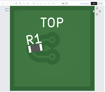
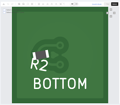
A good example is something so simple it needs no adjustment, a resistor. This is two resistors at 10 degrees rotation (as viewed from top), and sent to JLDPCB with a value of "10" in the rotation.
No standard within components
You may wonder why you may have to fettle the positions anyway, hence not noticing the bug. Well the reason is that there is, apparently, no standard for how components are "placed". Even though data sheets for components normally have detailed technical drawings showing the exact dimensions and outline, and even 3D models these days, there is no convention for component manufacturers providing an "origin" on their drawings, or even a "mid point", though "mid point" is at least something you may be able to work out on many. There is also no standard for which way is the "un-rotated" orientation of the component.
What is even more fun is that a component usually has three possible origins for its positioning, and some fabricators use different basis. Some may even use Mid and Pin 1 to define orientation, which is fine until pin 1 is in the centre of the device?
- Origin - some point on the technical drawing as a reference point, e.g. bottom left.
- Mid point - this at least is likely to be something you can work out for most components
- Pin 1 location - this is less simple - is it the mid point of the recommended SMD pad for pin 1 maybe? Or maybe the centre of the dot on the package marking pin 1?
This means that each fabricator makes up their own rules, on a per component basis. So you need a way to mark an offset X/Y and rotation on each component to match the fabricators rules. They are not even consistent - you would think a standard package, such as a small 8 pin IC, would always be the same orientation, but even that is not the case, even within one fabricator, it seems.
The big clue that the plug-in was wrong was that moving a correctly adjusted component from top to bottom broke it. By correcting the rotation on the bottom, it is now possible to make these "adjustments" part of the footprint for the component, so that whenever you use it, it will be placed correctly.
P.S. Don't get me started on poor quality technical drawings - i.e. those that are dimensioned with just slightly too few dimensions to work out all necessary points.
P.P.S. Don't get me started on poor quality 3D models. They look good, and many are stunningly accurate, and very useful, but they have an origin and orientation - this too is arbitrary, and often does not even have Z axis as "in/out of PCB when placed" - using these means manual fettling every damn time. If all components had a defined reference origin and orientation it could use that for the 3D model as well. Oh, and I have seen lovely detailed 3D models that actually do not match the footprint so look wrong!


No comments:
Post a Comment
Comments are moderated purely to filter out obvious spam, but it means they may not show immediately.